EXPLORE AVECAS
Engineering insights
Perspectives on silicon design, verification, embedded systems, and the engineering decisions behind them.
Nov 17, 2026
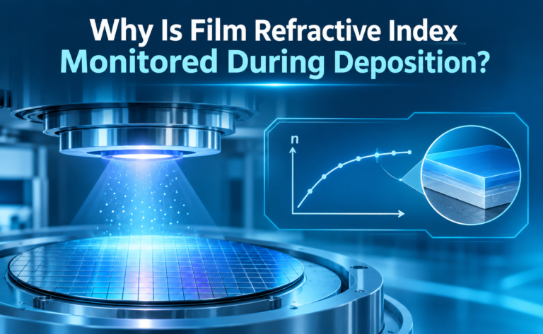
Thin-film deposition is a fundamental process in semiconductor manufacturing. It is used to form insulating layers, conductive films, dielectric materials, and optical coatings on…
Read article Why Is Refractive Index Monitoring Critical During Semiconductor Thin-Film Deposition? ↗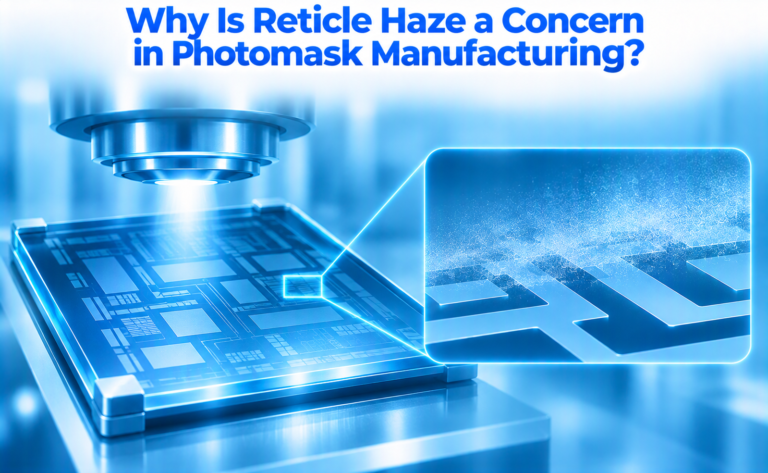
Nov 13, 2026
A photomask, also called a reticle, contains the precise circuit patterns used during semiconductor lithography. These patterns are transferred onto a photoresist-coated wafer through…
Read article Why Is Reticle Haze a Concern in Photomask Manufacturing? ↗
Nov 12, 2026
As semiconductor devices become smaller and more densely packed, individual transistors need to be electrically isolated to prevent unwanted current flow between neighboring components.…
Read article How Does Local Oxidation of Silicon (LOCOS) Form Isolation Regions? ↗
Nov 11, 2026
Extreme Ultraviolet (EUV) lithography enables semiconductor manufacturers to print extremely small features for advanced technology nodes. However, when contact holes are patterned at very…
Read article How Does EUV Stochastics Affect Contact Hole Formation? ↗
Nov 10, 2026
In advanced semiconductor manufacturing, forming accurate electrical contacts is essential for connecting transistor source, drain, and gate regions to the interconnect structure. These contacts…
Read article How Does Smart Contact Etch Stop Layer Technology Work? ↗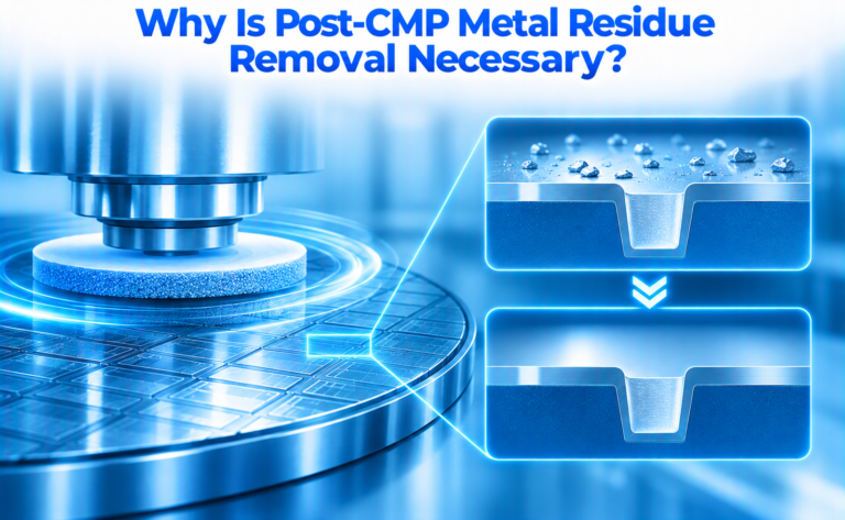
Nov 9, 2026
In semiconductor manufacturing, chemical mechanical planarization (CMP) is used to remove excess material and create a smooth, planar wafer surface. It is widely used…
Read article Why Is Post-CMP Metal Residue Removal Necessary? ↗
Nov 7, 2026
As semiconductor technology advances toward smaller transistor dimensions, controlling leakage current has become one of the major challenges in CMOS device design. Modern transistors…
Read article Why Is Gate-Induced Drain Leakage Important in Scaled CMOS? ↗
Nov 6, 2026
As semiconductor technology advances, the demand for faster, smaller, and more energy-efficient memory continues to increase. Conventional memory technologies such as DRAM and NAND…
Read article How Does Ferroelectric FET Technology Enable Non-Volatile Memory? ↗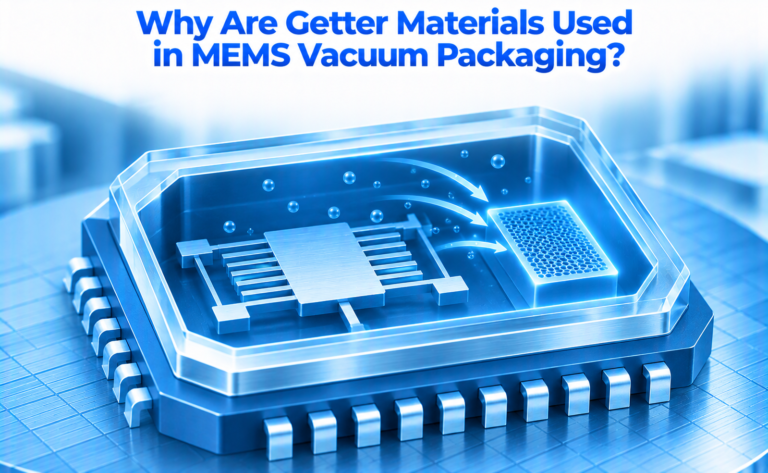
Nov 5, 2026
Micro-Electro-Mechanical Systems (MEMS) combine miniature mechanical structures with electronic components on a semiconductor substrate. Devices such as gyroscopes, accelerometers, pressure sensors, and micro-resonators often…
Read article Why Are Getter Materials Used in MEMS Vacuum Packaging? ↗
Nov 3, 2026
In semiconductor manufacturing, plasma etching is used to create precise openings such as contact holes, vias, and trenches in dielectric or other material layers.…
Read article Why Is Post-Etch Cleaning Necessary Before Metallization? ↗
Nov 2, 2026
Modern semiconductor chips are built through multiple patterning steps, where different layers are formed one after another on a silicon wafer. Each layer performs…
Read article Why Is Mask Registration Important in Multilayer Patterning? ↗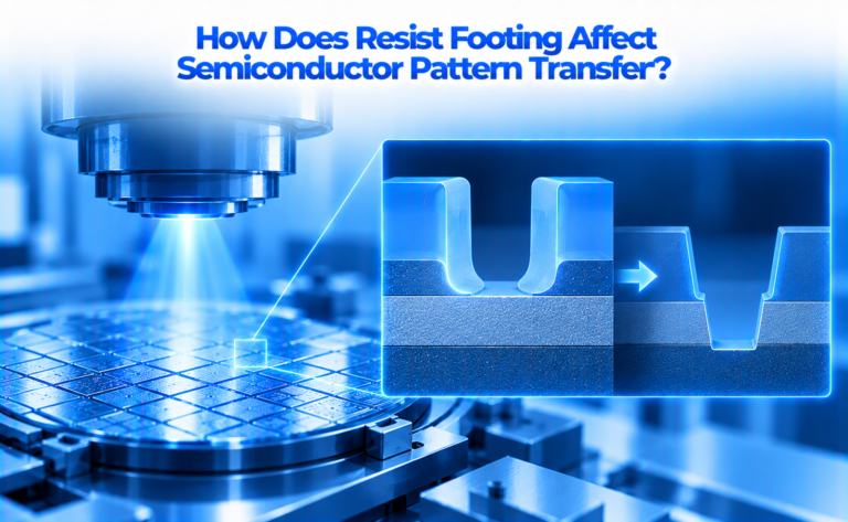
Oct 31, 2026
In semiconductor manufacturing, photolithography defines the tiny patterns that eventually become transistors, contacts, and interconnects on a silicon wafer. For accurate pattern formation, the…
Read article How Does Resist Footing Affect Semiconductor Pattern Transfer? ↗