EXPLORE AVECAS
Engineering insights
Perspectives on silicon design, verification, embedded systems, and the engineering decisions behind them.

Oct 16, 2026
As semiconductor devices become smaller and more complex, connecting billions of transistors through reliable metal interconnects has become a major manufacturing challenge. Modern integrated…
Read article Why Do Advanced Interconnects Need Barrier Layers? ↗
Oct 15, 2026
As semiconductor technology advances toward smaller process nodes, delivering power efficiently to millions or billions of transistors has become increasingly challenging. Modern processors, AI…
Read article How Does Backside Power Delivery Free Up Frontside Routing? ↗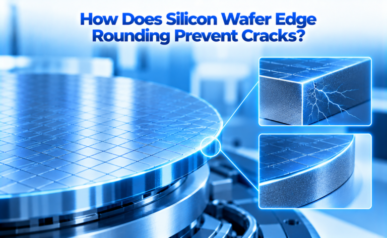
Oct 14, 2026
Silicon wafers are the foundation of modern semiconductor manufacturing. Before transistors, memory cells, and interconnect structures can be fabricated, the wafer must undergo several…
Read article How Does Silicon Wafer Edge Rounding Prevent Cracks? ↗
Oct 12, 2026
As semiconductor manufacturing advances toward smaller technology nodes, creating precise nanoscale patterns has become increasingly challenging. Modern integrated circuits require extremely narrow lines, tiny…
Read article Pattern Transfer Through Ultrathin Resist in Advanced Semiconductor Lithography ↗Oct 11, 2026
Scope an IC design engagement with clear inputs, acceptance criteria, ownership, review milestones, and reproducible handoff evidence.
Read article Planning a turnkey IC design project: a practical handoff checklist ↗
Oct 10, 2026
As semiconductor technology advances toward smaller transistors and increasingly complex device architectures, measuring microscopic features accurately has become essential for maintaining chip performance and…
Read article How Does CD-SEM Measure Tiny Features in Semiconductor Chips? ↗
Oct 9, 2026
As semiconductor devices become more powerful and complex, connecting multiple silicon dies with high bandwidth and low power consumption has become a major engineering…
Read article Why Are Microbumps Being Replaced by Finer-Pitch Bonding Technologies? ↗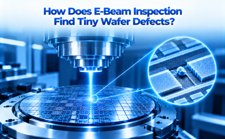
Oct 8, 2026
As semiconductor technology continues to scale, manufacturing defects that were once considered insignificant can become large enough to affect transistor performance, yield, or chip…
Read article How Does E-Beam Inspection Find Tiny Wafer Defects? ↗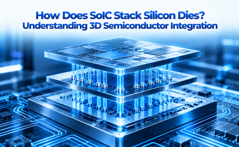
Oct 7, 2026
As semiconductor systems demand more computing power, higher bandwidth, and lower energy consumption, simply making individual transistors smaller is no longer the only path…
Read article How Does SoIC Stack Silicon Dies? Understanding 3D Semiconductor Integration ↗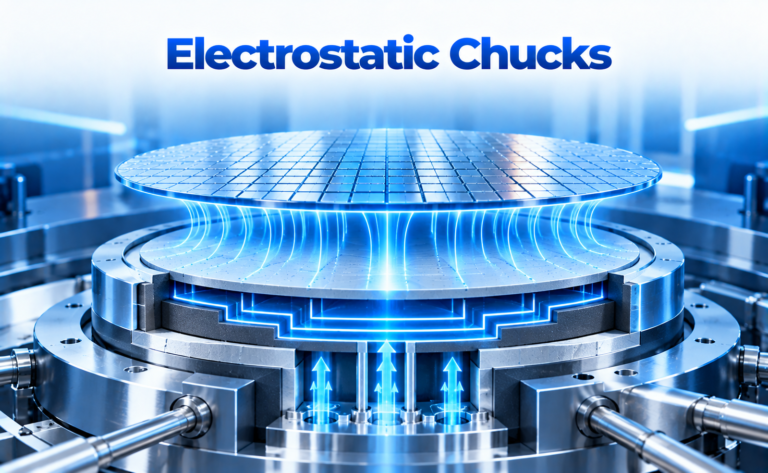
Oct 6, 2026
Inside a semiconductor fabrication chamber, a wafer must remain precisely positioned while processes such as plasma etching, deposition, ion implantation, and cleaning take place.…
Read article Electrostatic Chucks in Semiconductor Manufacturing: How ESCs Hold and Control Wafers ↗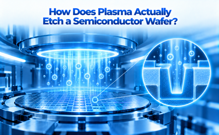
Oct 1, 2026
Modern semiconductor chips contain structures that are measured in nanometers, yet these structures must be created with remarkable precision across an entire silicon wafer.…
Read article How Does Plasma Actually Etch a Semiconductor Wafer? ↗
Sep 29, 2026
A modern semiconductor device is built from an intricate stack of extremely thin material layers. These layers may act as conductors, insulators, barriers, spacers,…
Read article How Does Thin-Film Deposition Build a Semiconductor Device? ↗